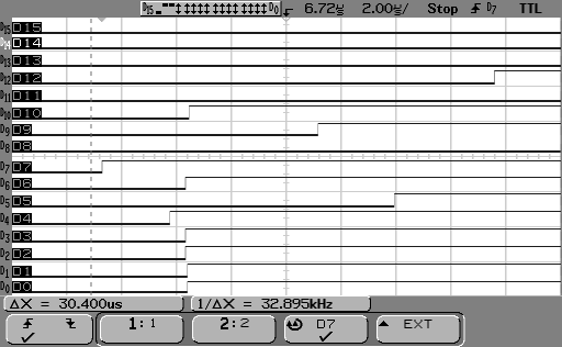
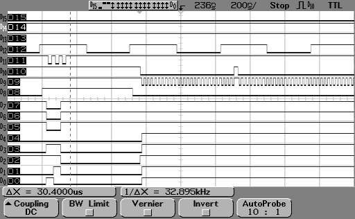
Close-up of initial powerup timing. D[7..0] are probably arbitrary at this point, and flipping as the ASIC comes up and sets its pins high-z?
| Pin |
Direction |
Name/Desc |
Comments |
| 1 |
Power |
Vdd |
3.0V; Connects to internal power plane |
| 2 |
I/O |
D7 |
(Pins 2-9 are parallel data out) |
| 3 |
I/O |
D6 |
|
| 4 |
I/O |
D5 |
Pulled up by 100k resistor. |
| 5 |
I/O |
D4 |
|
| 6 |
I/O |
D3 |
|
| 7 |
I/O |
D2 |
Pulled up by 100k resistor. |
| 8 |
I/O |
D1 |
Pulled up by 100k resistor. |
| 9 |
I/O |
D0 |
Pulled up by 100k resistor. |
| 10 |
O |
SYNC | For me, goes HIGH to indicate the next line will contain valid data. It should probably go high at the end of every line, since every line should probably contain valid data, but I'm only getting data every 96th line clock. (Normally low; single 500ns pulse repeating at a rate of 2MHz when controlled by camera.) |
| 11 |
Power |
GND |
|
| 12 |
I |
BYTECLK |
Rising edge clocks next byte of the current line onto D[7..0]. |
| 13 |
I |
OE\ |
LOW enables data output on D[7..0] |
| 14 |
I | INCLK |
Falling edge clock command byte on D[7..0] into the imager. D[7..4] are the configuration register address. While camera running, normally-high signal, with a very quick "01010" pattern (100nS from the starting edge of the first '0' to ending edge of last '0') occuring once every 20KHz when in camera. |
| 15 |
Power | GND |
|
| 16 |
I |
LINECLK | The
PV2's processor pumps a 2MHz clock into this pin at pretty much all
times. For me, clocking it just after startup (OE\ disabled) will yield
a pulse on SYNC every 10th clock or something. Appears to advance to
next line (when clocked 96 times... watch SYNC to see if line is valid) |
| 17 |
Analog bias in? See notes below | ??? |
High analog voltage (near 3.0V rail) in camera. Externally tied to pin 24. |
| 18 |
I? |
??? (RESET\?) |
HIGH in camera |
| 19 |
Analog, see connection notes below | ??? |
In camera, seeing about 2.8V on this pin. Smoothed by a decoupling capacitor to GND. |
| 20 |
Analog out, seemingly NC |
??? |
In camera, about 1.3V on this pin. Output smoothed by a decoupling capacitor to GND. |
| 21 |
Analog out, seemingly NC | ??? |
In camera, about 0.84V on this pin. Output smoothed by a decoupling capacitor to GND. |
| 22 |
Power |
GND |
My, SMaL's imager is really full of grounds. |
| 23 |
Analog out, seemingly NC | ??? |
In camera, about 1.6V on this pin. Output smoothed by a decoupling capacitor to GND. |
| 24 |
Analog bias in? See notes below | ??? |
High analog voltage (near 3.0V rail) in camera. Externally tied to pin 17. They are smoothed by a decoupling capacitor to GND. |
Notes for pins 17-24:
Pins 17 and 24 are tied together on the camera PCB.
Pins 19, 20, 21, 23, and 24 (and 17, by virtue of the above) have a
bypass capacitor to ground. I haven't measured the value, but something
in the realm of 100nF is a safe bet. It doesn't seem to critical to
know at this stage; maybe when I have an image out of this thing I can
play with that to clean up noise.
Pin 17/24 is connected to a (digital?) signal line on the ASIC via a
100k resistor. That same signal line is connected to pin 19 via a 30k
resistor. (So, 17/24 and 19 are in effect connected together through
130k, but this probably isn't important.) When I get slightly more
ambitious (and have access to a scanner again) I'll draw a little
diagram of all this.
Initialization:
Appears to be as follows:
Raise OE\
Raise BYTECLK
Raise LINECLK
Raise pin 17/24
(wait a little while)
Raise INCLK
(wait a long time)
Raise pin 18 (RESET\ ?)
Configuration Registers:
Configuration appears to be set by clocking in bytes on D[7..0] using
INCLK. D[7..4] appear to be the address of the configuration register,
while D[3..0] contain the configuration data itself. The function of
each register remains unknown. Configuration registers are set after
performing the 'Initialization' step above.
| Address |
Data (supplied by PV2) |
Description |
| 0x01 |
1111 |
? |
| 0x02 |
1110 |
|
| 0x03 |
0101 |
|
| 0x04 |
1000 | |
| 0x05 |
1000 |
|
| 0x06 |
0100 |
|
| 0x07 |
0000 |
|
| 0x08 |
1111 |
|
| 0x09 |
1101 |
|
| 0x0A |
0111 |
|
| On frame start only: |
The following occur on frame (or line? Analyser is hard to trigger) start, NOT initialization |
|
| 0x0B |
0000 |
|
| 0x07 |
0000 |
|
| 0x00 |
0111 |
Logic Analyser:
I decided to wire my test jig back
up to the camera (rainbow wire and epoxy, whee!) and attach the whole
mess to my work's Agilent scope, which doubles as a logic analyser. It looked like a pin cushion.
The analyser probes were attached in order of 'interesting pins',
starting with Pin 2 of the imager being D0 of the analyser. It turns
out Pin 2 (D0 here) is actually the imager's D[7], and D7 on the
analyser (Pin 9) is actually the imager's D[0]. In other words, D7 thru
D0 below are the imager's parallel data bus flipped backwards, and the
rest of the numbers are fairly arbitrary. Analyser D15 is unconnected.
So to recap:
| Analyser signal |
Pin on imager |
Name (if known, from table above) |
| D0 |
2 |
D[7] |
| D1 |
3 |
D[6] |
| D2 |
4 |
D[5] |
| D3 |
5 |
D[4] |
| D4 |
6 |
D[3] |
| D5 |
7 |
D[2] |
| D6 |
8 |
D[1] |
| D7 |
9 |
D[0] |
| D8 |
10 |
SYNC |
| D9 |
12 |
BYTECLK |
| D10 |
13 |
OE |
| D11 |
14 |
INCLK |
| D12 |
16 |
LINECLK |
| D13 |
17 |
|
| D14 |
18 |
(RESET?) |
The camera was then turned ON and left sitting idle. The imager appears
to still be clocked in this state (and line data changes in response to
light changes in front of the imager), so I'm guessing it's actually
acquiring images during that time, and captured some traces:
Close-up of initial powerup timing. D[7..0] are probably arbitrary at
this point, and flipping as the ASIC comes up and sets its pins high-z?
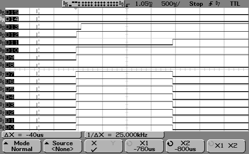
Zoomed out view of initial powerup. Note D14 hasn't flipped yet, but it soon will.
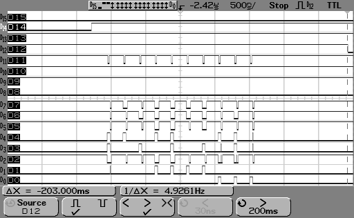
Now D14 (believed to be RESET) flips, and the PV2 begins clocking
configuration data into the imager. Notice that on D0 ~ D3 (D[7..4] on
imager) the monotonically increasing binary value starting with 0001
and going up to 1010. These bits then are almost certainly a
configuration register address.
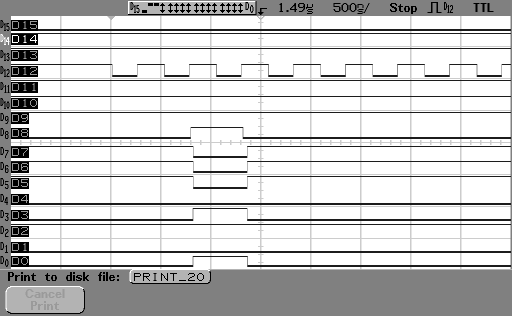
Shortly after, the line clock starts flipping. Since the imager hasn't
pulled SYNC high yet, the camera doesn't bother clocking the BYTECLK
since the line data isn't valid anyway. But wait, it DID pull SYNC high
for a moment! Maybe the camera knows something we don't.
This might be the start of a frame. But it might do this other times (every line, or every nth
line) too. It's hard to say, since the analyser's triggering isn't very
complex. Note D12 (LINECLK) toggles at a constant rate, even while
bytes are being read out. Also note 3 bytes clocked into the
configuration registers, with the order and data as shown in the
Configuration Registers table above. Maybe this starts/stops an image
acquisition period? Or resets a data pointer to start of frame? Don't
know. Finally, note that there was a pulse on D8 (SYNC), so the camera
starts clocking BYTECLK to read out data. (There doesn't appear to be
any yet, but it does show up eventually. Unfortunately I don't have a
trace of this.)
Guessing method(s):
Signals described were passively probed in-circuit with a digital
storage oscilloscope while camera 'idle' (strangely, it appears to be
reading the imager continuously during this time); but later I
desoldered the imager, breadboarded it and started trying to talk to it with a PIC.
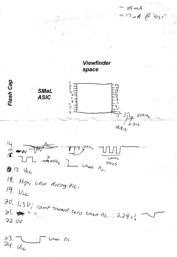
For now the imager is covered with a piece of plastic and Scotch tape
to keep dirt, scratches and my greasy fingerprints off it until I've
got the communications down well enough to read an actual image out of
it. The chip at right is an RS232 driver for bootloading new code onto
the micro. (I'm going to spend $200 on a programming puck when I can
bootload? Puck no, james!) One thing is for sure, I'm definitely
wreaking havoc with any possible timing requirements by reading data
out (to my PC over RS232) at about 1 line per second; since the
official byte clock is something like 50MHz.
After identifying output enable, I tried gently pulling the voltage
of each unknown pin up & down to determine whether they were inputs
or outputs. Results (if known) are in the table above.
Old Stuff: A picture and some
descriptions of what the signals on each line look like. A lot of this
is kind of obsolete; trust the above if in doubt.
Unless otherwise indicated, signals were measured with the camera 'idle'...oddly enough, the imager is being continuously read during this time, and only 'goes dead' in the couple seconds immediately following a shutter press.
"xxx when pic." indicates the signal present in the couple seconds following a shutter press, when picture data is supposedly being acquired, then processed, for those signals I bothered measuring during a picture-taking. Due to the Herculean effort involved in trying to trigger a 'scope while holding onto probes and trying to press a shutter button at the same time, the "...when pic." descriptions for data lines are very unlikely to represent what is actually happening during the final image acquisition - they mostly represent lines simply "going dead" while the ASIC is busy processing the image.
Handwritten text contains my own personal shorthand of sorts, which may be confusing and inaccurate. (For example, some pins labeled "Vcc" are really just logic high signals, and for some reason I wrote 'active high' to mean 'idles high'. Maybe I was just 'active high' on solder fumes.) When in doubt, use the text descriptions below.
Readable text description of signals follows the handwritten scrawl and poorly-drawn signal traces.
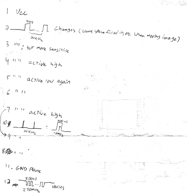
1. Vdd? 3.3v; Connects to internal plane
2. Digital I/O (D7?) : When nothing interesting happening in front of
the imager, data consisted of a normally-low signal with a single ~
44ns pulse repeating at a rate of 20KHz. Data 'got busy' with a
changing image in front of the imager. Similar results for signals
marked D[6..0] below; they seemed to get busier or "more sensitive"
down the line, hence the guesses as to bit-significance. Unfortunately
I don't have the facilities to actually analyze / record data moving
this fast. Some of the signals seemed to default to a high value
instead of a low one.
3. D6? (mostly low)
4. D5? (mostly high)
5. D4? (mostly low)
6. D3? (mostly low)
7. D2? (mostly high)
8. D1? (mostly high)
9. D0? (mostly high)
10. (Sync?) Normally low; single 500ns pulse repeating at a rate of 2MHz
11. GND
12. Normally high - bursts of 50MHz clock signal from ASIC to imager
followed by what appeared to be varying lengths of idle (high) signal.
Number of clock pulses per burst couldn't be measured with my
equipment, but there were lots of 'em. This is verified as a required
data clock to the CMOS; cutting it results in the ASIC reading in image
data of all 0s.
13. Clock-like signal with non-uniform duty cycle (high 28.8uS; low 21.2uS), frequency of 20KHz
14. (Another sync?) Normally-high signal, with a very quick "01010"
pattern (100nS from the starting edge of the first '0' to ending edge
of last '0') occuring once every 20KHz.
15. GND
16. Clock-like signal; frequency 2MHz. Low when pic.
17. Analog voltage; tied to pin 24
18. High; low when pic.
19. Analog voltage? ~ 2.8V
20. Analog voltage ~ 1.3V; exponential decay to 0 over the course of ~ 2.28 seconds when pic.
21. Analog voltage ~ 0.84V
22. GND
23. Analog voltage ~ 1.6V
24. Analog voltage; tied to pin 17